AVR Glitch: Modifying Code Execution Paths Using Only Voltage
Take a look at this simple code:
ctr = 0;
for(i=0; i<500; i++){
   for(j=0; j<500; j++){
     if (j % 100 == 0) {
       ctr++;
     }
   }
 }
At the end of this execution, there should only be one feasible value of ctr: 2500. The program takes no other input that could cause any deviations from a straightforward series of instruction executions and a very predictable output.
Moving away from theoretical execution to actual hardware, you’d likely still expect the same answer, despite infinitely complicated operating systems and layers upon layers of abstraction at the hardware layer.
What follows is a very basic introduction to the idea that intentionally manipulating only the voltage of a microprocessor can affect the outcome of very simple arithmetic and logic in moderately repeatable and sometimes controllable ways.
This is far from new material; glitching was used to unlock the Xbox360 (among other things) and has already been covered extensively in prior research. This is an attempt to get hands-on for minimal startup cost and effort – an Arduino Uno and a $21 FPGA.
The Plan
There are a number of invasive and non-invasive attacks that attempt to disrupt a chip; the two most simple being clock and power glitching. We’re going to go with power glitching, where we’ll simply drop the voltage supplied to the microcontroller for a very brief period of time, quickly raise it back up to operating voltage again and see what happens.
This is going to be very random and not particularly well targeted – we’re not trying to pull off an incredible feat of hacking but instead just demonstrate the correlation between tinkering with Vcc and code execution paths. We’re not even going to try the glitch and a particular time; we’ll just keep doing it and watch what happens.
Digital logic circuits tend to operate at very high speeds; clocks in the MHz and up range mean that somewhat specialized tools are required for interacting with these devices. Oscilloscopes and Logic Analyzers are typical go-to tools for observing signals inside a digital circuit, but we actually want to be sending signals, not just reading.
For this, we’ll use a Field Programmable Gate Array. It’s essentially a chip that we can wire up as a digital circuit however we like, and have it run at full silicon speed. The tool used here is an iCEstick by Lattice Semiconductor which comes in at a fairly affordable $21 and just plugs straight into USB. Even better, there’s a fully open-source toolchain which makes setup really easy and lightweight. The FPGA can be programmed using a schematic editor or via a Hardware Description Language (HDL); I’m going to write the very tiny amount of required HDL code in Verilog.
Test Setup
The hardware setup is incredibly simple: we load the target code up to the arduino and remove the ATmega AVR chip onto a breadboard. The breadboard is used so we can get inline with the actual power supply wires, where we’ll drop in a transistor to give us the ability to turn power on and off.
That transistor will be driven from an output on the FPGA, which will be loaded up with some simple Verilog code to create an output signal that goes low for a brief period of time on a regular basis. The FPGA will be switching the AVR power supply on and off as it chooses, and given the 12MHz clock of the FPGA, will allow very fine grained glitch pulses down to the low hundreds of nanoseconds (1/1,000,000,000 of a second).
Make sure you’ve loaded up the Arduino code in the IDE and uploaded it to the Arduino. Check the Serial Monitor to make sure it’s sending regular messages which look something like:
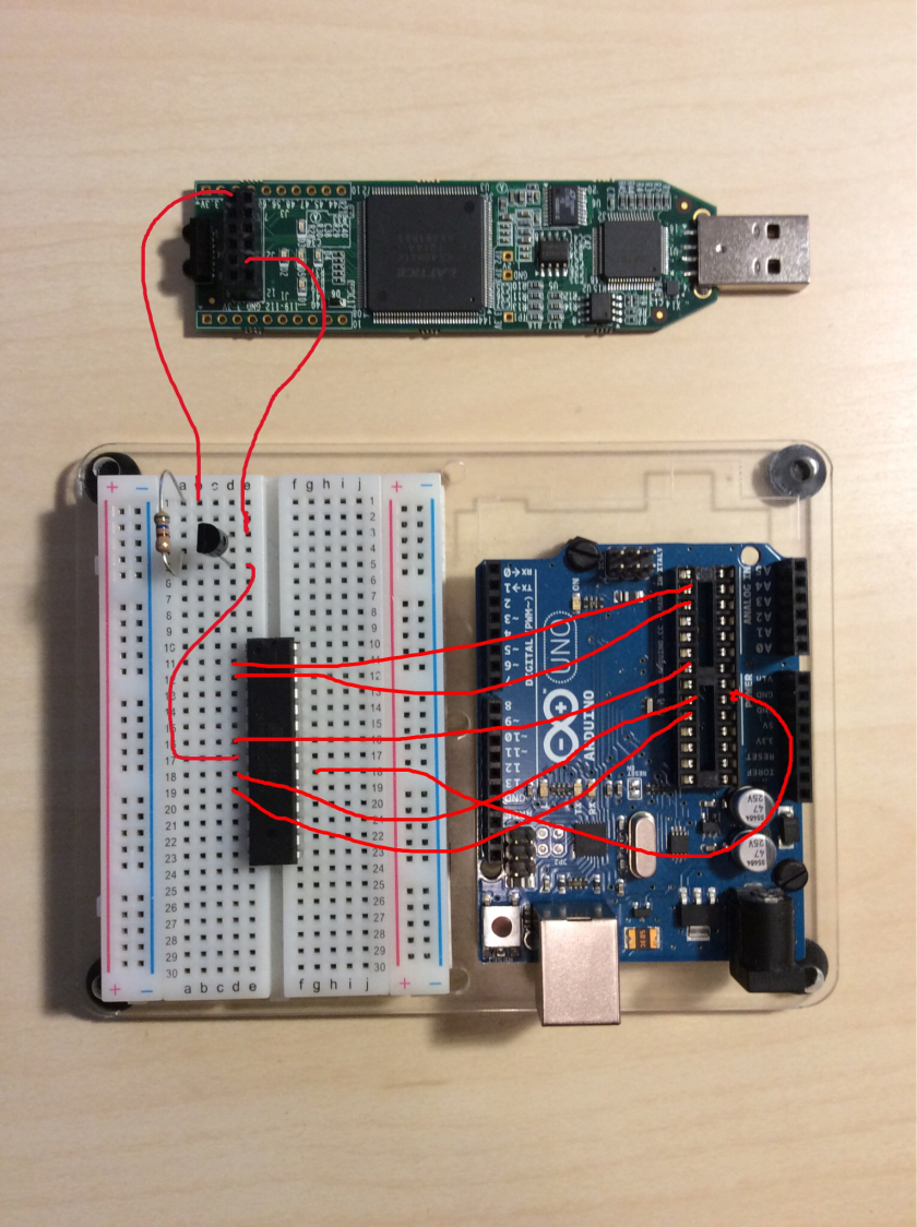
500 + 500 = 1000 ctr: 2500Here’s a diagram of how the hardware should be wired up:

The only components other than a bunch of connector wires are a transistor and a resistor. I’m no electrical engineer, so I just found a P2N2222A and a 560Ω resistor and they seem to work. I have no idea if the resistor is even required; but it works.
When shifting the AVR from its Arduino socket to the breadboard, a few pins can be wired directly: 20 (AVCC), 2 & 3 (for serial IO), 7 (VCC), and 9 & 10 for clock signal.
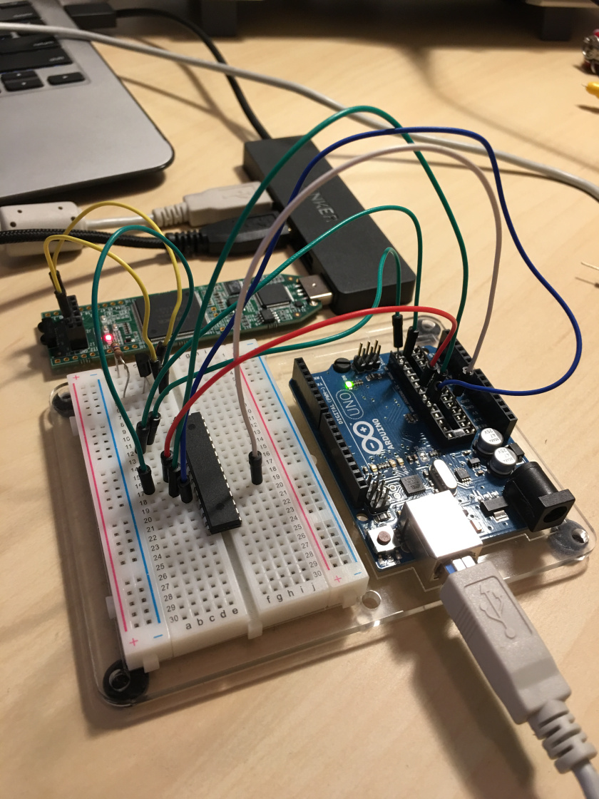
The glitch signal coming from J1_1 on the FPGA connects into the base of the transistor via the resistor, while one side of the transistor is hooked up to the MCU’s GND, and the other to the FPGA’s own GND.
It may look something like this:

Now it’s time to program the FPGA. If you follow the guide here, you should be able to have the prereq toolchain up and running very easily (I’m on Ubuntu 16.04 and it was a walk in the park). You should be able to build and upload the blink.v Verilog with a simple ‘make’ in the code directory. If you’re suspecting it’s called blink.v because it was my first ever Verilog project and started out as blinking an LED, you’d be one hundred percent correct.
Results
With any luck, you’ll see the debug output being sent back to the Arduino IDE Serial Monitor (or whatever you’re using to keep tabs on the serial IO). Instead of the correctly calculated values, you should see something more like:
500 + 500 = 1000 ctr: 2500
500 + 500 = 1000 ctr: 2501
500 + 500 = 1000 ctr: 2499
500 + 500 = 1000 ctr: 3044
500 + 500 = 1000 ctr: 4000
500 + 500 = 1000 ctr: 2500
500 + 500 = 1000 ctr: 2500
500 + 500 = 1000 ctr: 2500
500 + 500 = 1000 ctr: 2500
500 + 500 = 1000 ctr: 2500
500 + 500 = 1000 ctr: 2154
500 + 500 = 1000 ctr: 2000
500 + 500 = 1000 ctr: 2379
500 + 500 = 1000 ctr: 2500
500 + 500 = 1000 ctr: 500
500 + 500 = 1000 ctr: 500
500 + 500 = 1000 ctr: 500
500 + 500 = 1000 ctr: 1871
500 + 500 = 1000 ctr: 1500
500 + 500 = 1000 ctr: 1500
500 + 500 = 1000 ctr: 1500
500 + 500 = 1000 ctr: 11252
Glitching (in particular in this manner) can have a fair degree of randomness, so output can vary wildly. You can also expect some poorly timed glitches to cause the AVR to fully reset.
What’s fascinating about this is the manner in which the processor typically continues normal execution just fine, but with particular data or instructions not as they should be. This type of manipulation can and regularly is honed into a much more precise attack to extract data or exploit hardware to gain access, as seen plenty previously.
The Verilog code as it is has a major drawback; the timing values are hardcoded and the programming step takes a significant amount of time. If you’re not seeing any results, the GLITCH_DURATION variable can be modified; a higher value means the AVR power will be dropped for longer and should increase the chances of an adverse effect, but could also result in a full reset.